VLSI
VLSI 1: 32-bit Silicon CMOS Adder-Subtractor
November 2025 - December 2025
A full-custom 32-bit CMOS adder-subtractor in 0.25 μm n-well silicon — 2's-complement arithmetic, one full adder clocked across 32 bits, 970 transistors.
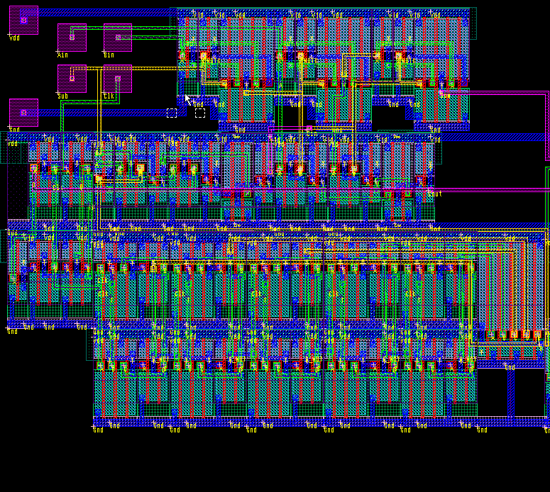
The Architecture
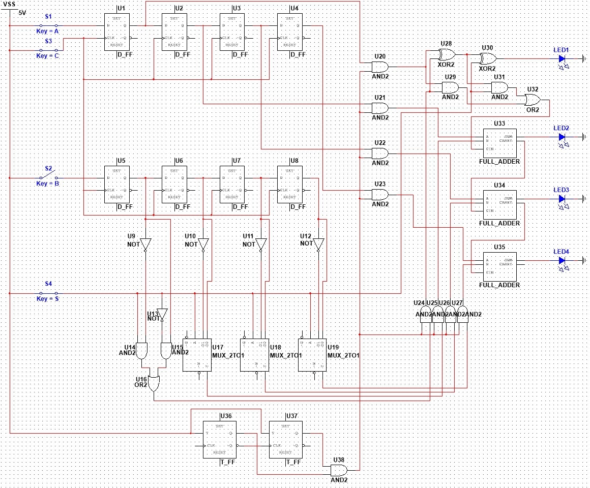
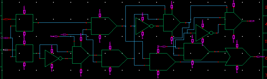
Bryan Galecio and I designed this for ECE 658 — VLSI Design at NJIT. Subtraction is 2's complement: invert B and add one. A single adder then does both add and subtract. A and B come in serially on two pins to keep the chip under 40 pins; a 5-bit T-flip-flop counter times the 32 clocks.
The first architecture used two 32-bit shift registers and a 32-bit ripple-carry adder — 3,696 transistors. The version we laid out uses one full adder, one 32-bit result register, and a mux that feeds the add/subtract select as the first carry-in. That cut the count to 970 transistors.
Custom Cells
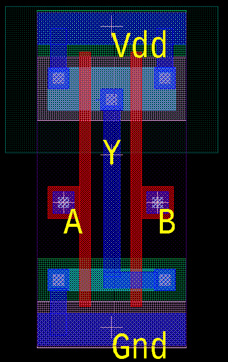
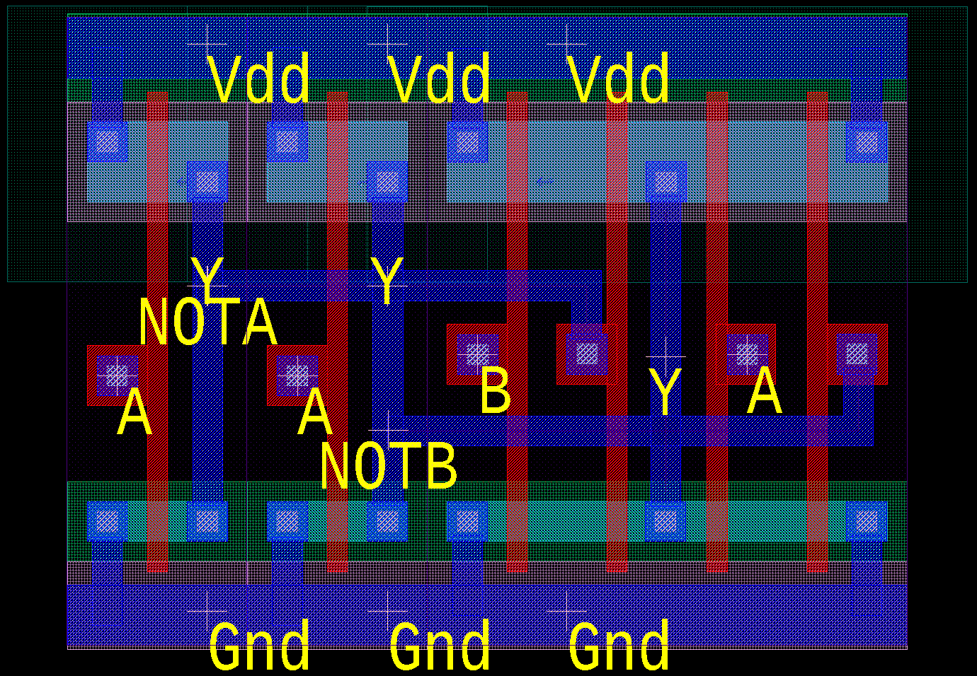
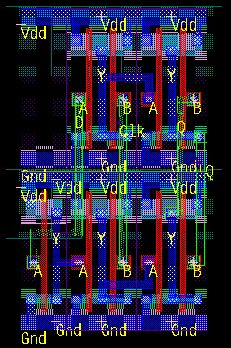
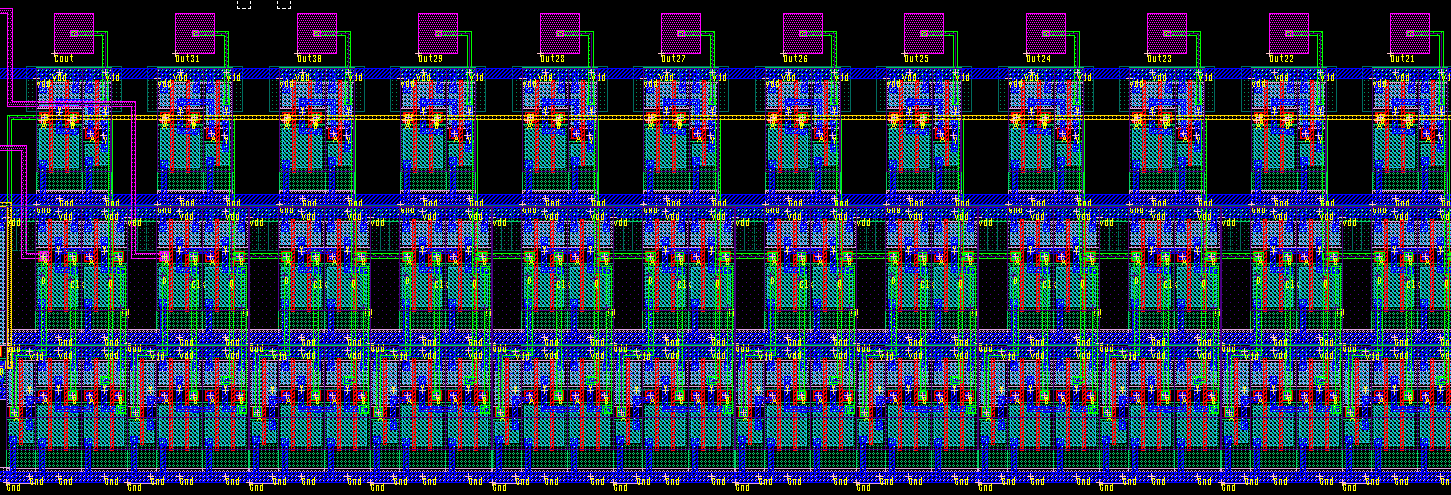
Every gate is transistor-level in Tanner S-Edit and L-Edit, not a standard-cell library: INV, NAND2, NAND3, NOR2, XOR2, then D flip-flops, T flip-flops, a 2:1 mux, and a full adder. Bryan laid out a couple of the small gates and handled the simulations and documentation; I did most of the small gates and all of the large cells — the flip-flops, mux, and full adder. Cells share a common height so the power rails line up. The finished layout is 363 μm × 46 μm on four metal layers.

Verification
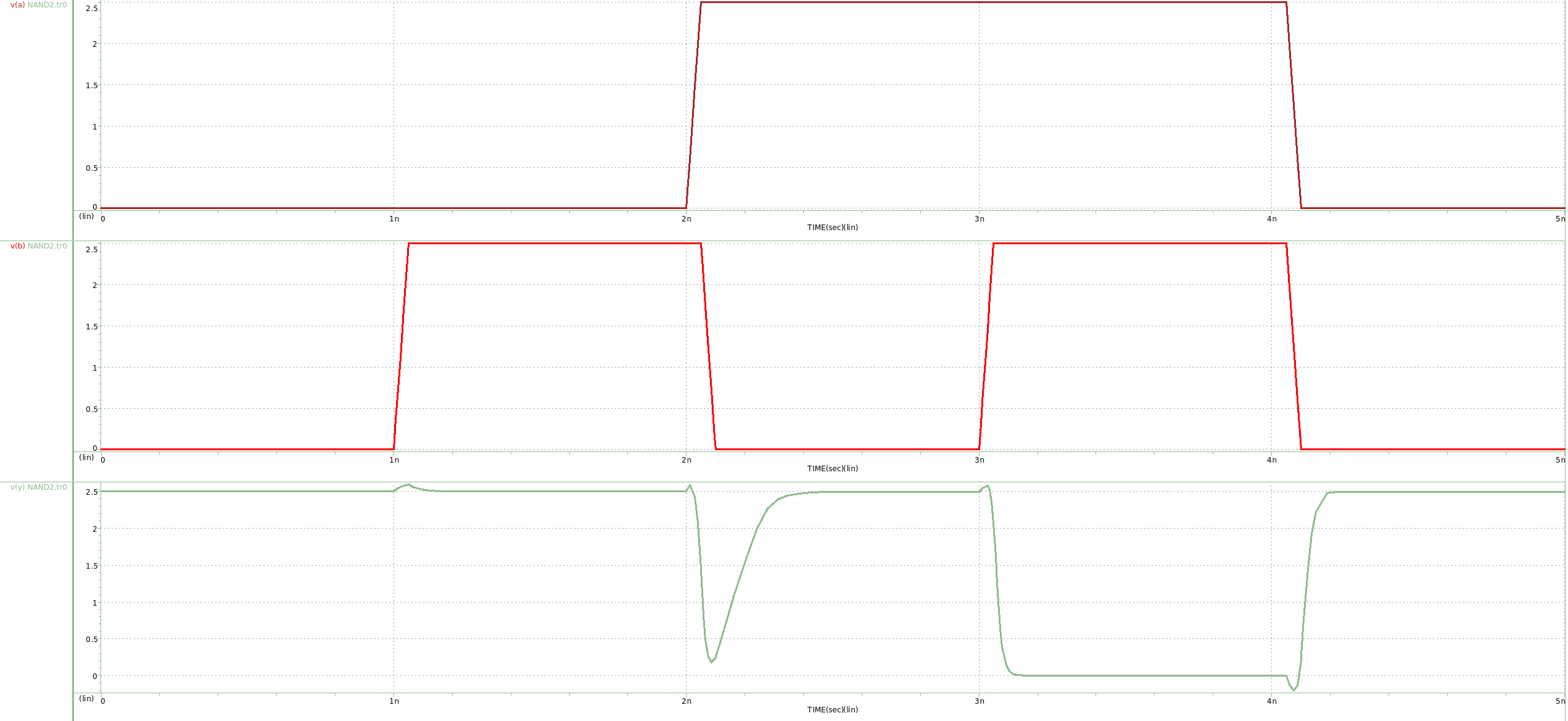
We checked the architecture in Multisim on 4-bit and 8-bit prototypes before drawing the 32-bit schematic. Bryan ran the HSPICE simulations in WaveView. DRC was not available on the university machines, so we could not extract parasitics or run post-layout simulation.
Result
I integrated the full 32-bit datapath onto 39 pins, including 32 parallel sum bits, serial A and B, add/subtract select, carry-out, clock, VDD, and GND. The iterative architecture cut transistor count by about 74% versus the first parallel design. This stayed on the university tools — schematic, layout, and cell-level HSPICE — not a fabricated part.